
Printed circuit boards (PCBs) and Integrated Circuit chips make the modern world we know possible. As commonplace as printed circuit boards are in our world, many people still misunderstand their design and function in tech items today. There’s a certain cloak of mystery surrounding PCBs and their purpose to provide component connection within electronic pieces. The PCB industry is steadily on the rise as present-day technology expands and gains traction with fresh innovations.
Difference Between a Chip and PCB
A PCB is a fiberglass plate with copper traces to connect components together. A chip is a set of electronic circuits on one small flat piece (or “chip”) of semiconductor material, usually silicon. A chip is then placed in a housing, commonly a small black box with metal pin connectors. Chips are smaller scale than PCBs, and usually more sophisticated with a specific function. Chips might be placed on a PCB as part of an aggregated multi-function device. Companies such as Apple have a much more sophisticated chip manufacturing processes and are putting more functions in their chips with the CPU as they move away from Intel.
What do you know about the subject of PCBs? Unless you’re a designer or assembler, you might believe the circle of myths floating around about these intricate circuit boards. PCB design is fairly complex yet not too complicated if you’re interested. To separate fact from fiction, we’ve compiled a list of the most common misconceptions about PCB design.
Myth 1: The Same Design Rules Apply to All Boards
The basic components and makeup of PCBs are similar to one another. Typical boards will have around two to four layers with a certain thickness level and copper weight. These foundational layers include a substrate, copper, solder mask, and silkscreen. The silkscreen printing of PCBs is for informational and functionality purposes. That said, printed circuit boards are not all the same in design.
The fabrication method and assembly process are all dependent on the board’s primary functions. PCB design is unique; you can consider the process a technical art form of putting various puzzle pieces together. Standard settings and rules don’t ensure successful results for all designs upon assembly.
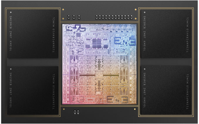
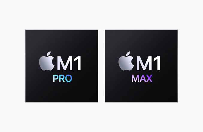
Apple’s Trend Toward More on Chip
The motherboard of a computer is the main Printed Circuit Board of a computer with a chipset that involves data flow for the CPU (Central Processing Unit), memory (RAM) and peripherals, etc. Apple® — using its own silicon-based chips instead of Intel chips — has developed M1, M1 PRO and M1 MAX chips with a System-on-a-Chip concept that combines more component functions, such as chip memory (DDR4 memory), I/O chip, Security (Apple T2), CPU and Thunderbolt controller within the M1 chip. The result is a gain in speed and savings in in electric power.
Myth 2: Component Placement Doesn’t Matter Much
Another one of the most common misconceptions about PCB design revolves around component placement. Again, not all design rules apply to specific PCBs, but careful consideration of part placement is the key to circuit performance. Designers can’t simply place components just anywhere on a board, and they can’t group similar parts together to try to save space. They also have to consider heat and electrical overload. As chips rise in sophistication and gain more functions, there is less wiggle room for customization or even repair because there are less components on the circuit board. Hopefully chips will have rock solid reliability.
To clarify, think about a printed circuit board three-dimensionally. Designers must consider the physical height of components as much as their size and width. Each PCB component must sit in a specific location and position for quality assembly. At the end of the day, this process is essential to maintain a functional electrical scheme that doesn’t overheat and saves on power consumption. Otherwise, today’s tech would fail over and over again.
Myth 3: Printed Circuit Boards Are Not Eco-Friendly
There’s definitely some truth to the negative Eco-Friendly issue, but there are efforts to improve harmful effects on the environment. You may have heard that designing, assembling, and manufacturing PCBs is not environmentally sound. According to the EPA, the wastes resulting from printed circuit board manufacturing are associated with five types of processes: cleaning and surface preparation; catalyst application and electroless plating; pattern printing and masking: electroplating; and etching. The wastes include airborne particulates, spent plating baths, waste rinsewater, and other wastes. Additionally, most electronic devices don’t last forever, so there is a need to recycle material or reduce waste in the landfills. This does mean being tech-savvy while using products from careless manufacturers is harmful to the environment. Ethical sustainability in the electronics world involves non-toxic fabrication materials and/or using materials that are recyclable.
Going back at least to 1990, the working definition used by the EPA was that waste minimization consists of source reduction (preventing the generation of waste at its point of origin) and recycling. Of the two approaches, source reduction is usually considered preferable to recycling from an environmental perspective. Treatment of hazardous waste is considered an approach to waste minimization by some states but not by others, according to the EPA.
Future strides by engineers involve efforts to make biodegradable board design a possibility on the horizon. Greener manufacturing technology is also around the corner.
Meanwhile, Apple says their goal is to one day source all of the valuable resources required to make an iPhone only from renewable and recycled alternatives. Apple report the company has recently transitioned to 100% recycled gold in the plating of the main logic board and the wire in the front camera and rear cameras. Apple now uses 100% recycled rare earth elements in all magnets, 100% recycled tungsten in the Taptic Engine, and 100% recycled tin in the solder of the main logic board and battery management unit.
The more common and ubiquitous PCB design still remains an integral part of our tech industry — from electric blanket controllers to key fobs. Regardless of whether you’re a user or designer, it’s wise to gain further perspective about the topic to choose a device with more speed from your computer.
^^ MOBILE? USE VOICE MIC ^^
facebook …
Please ‘LIKE’ the ‘Arlington Cardinal Page. See all of The Cardinal Facebook fan pages at Arlingtoncardinal.com/about/facebook …
Help fund The Cardinal Arlingtoncardinal.com/sponsor
20240105-1435future
THANKS FOR READING CARDINAL NEWS
